TOKYO, Nov 7, 2024 - (JCN Newswire) - Hitachi High-Tech Corporation ("Hitachi High-Tech") and The University of Tokyo ("UTokyo") have been conducting joint research ("this research") into practical applications of high-resolution Laser-PEEM(1) developed by UTokyo in the semiconductor manufacturing process. This research will be presented at MNC 2024 (International Microprocesses and Nanotechnology Conference 2024), which will be held in Kyoto Prefecture from November 12 to 15, 2024.
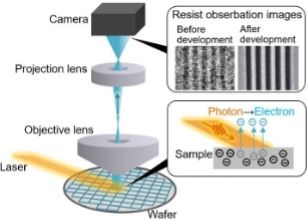
 Overview of Laser-PEEM
Laser-PEEM can be faster image analysis compared to SEM(2) used in the semi-conductor wafer manufacturingprocess, and observation of the chemical information of materials and the non-destructive observation of three-dimensional structures on the nano-level used high- resolution technology developed by UTokyo. In this research, we conducted trials on the application of Laser-PEEM in the semiconductor field and have verified its effectiveness.
We will continue to conduct research in collaboration with UTokyo by understanding the needs of semiconductor manufacturers to help resolve issues in the manufacturing and shipping processes.
(1) Laser-PEEM: Laser-Photo Emission Electron Microscope
(2) SEM: Scanning Electron Microscope
Background
As semiconductor device performance has improved with the progress that's been made in miniaturization and high integration, at present, nano-level circuit patterns are being formed using extreme ultraviolet (EUV) lithography. Asdevices become increasingly miniaturized and highly integrated, changes in 3D processing precision of circuit patternsand localized material properties in the manufacturing process have come to have a greater impact on device performance than ever before. For this reason, multi-point and varied inspections and measurements are becoming essential, and the need for improved inspection throughput is expected to continue to increase going forward.
Hitachi High-Tech has been conducting joint research with UTokyo since 2020, which developed the high-resolutionLaser-PEEM technology, with the aim of resolving further issues facing customers by leveraging Hitachi High-Tech's expertise in supporting semiconductor manufacturing through high reproducibility and throughput.
Details of This Research's Trials Using the Features of High-resolution Laser-PEEM
1. Quick nano-scale observation
Laser-PEEM irradiates the entire observation target with a laser instead of an electron beam, and obtains the observedimage by capturing the electrons emitted from the observation target with a camera. This research has verified that, using this method, it is possible to obtain a wider area of high-resolution data at once, thereby contributing tosubstantially shortening the inspection process compared to a SEM, which scans using an electron beam.
2. Enables the observation of various chemical information of materials
The semiconductor manufacturing process consists of three main processes: resist coating, exposure, and development. In order to inspect the shape of circuit patterns, we currently inspect the uneven patterns formed on thewafer surface after development. It is believed that yield could be improved if it were possible to inspect what are called latent image patterns, which are formed immediately after exposure and are chemically etched with no irregularities on the actual surface. In this research, we applied Laser-PEEM to latent image pattern observation anddemonstrated that it was possible to observe them at high resolution and with high throughput. This functionality is a technique that was not possible with SEMs, and we anticipate this could lead to the creation of new inspection markets going forward.
3. Enables non-destructive observation of nanostructures
Laser-PEEM is capable of sensing at depths of approximately 10 to 100 nanometers, and we have demonstrated that it is able to "look through" and see whether defects are present in wafers and what caused them in a non-destructive manner. This makes it possible for the previous work of processing wafers to analyze the cause of faults to now be carried out non- destructively. We also expect to see more advances in moving to three-dimensions going forward,thereby contributing to reducing the workload involved in processing, as well as more accurate analysis.
Future Outlook
By providing inspection and measurement equipment using electron beam technology and optical technology, Hitachi High-Tech continues to respond to our customers' various processing, measurement and inspection needs in the development and mass production of semiconductor devices. Looking to the future, the combination of this high-resolution technology developed by UTokyo and Hitachi High-Tech's automation and stabilization technology, together with an extensive customer network, will open up new possibilities for applying high-resolution Laser-PEEM in inspections and measurements in the cutting-edge semiconductor manufacturing processes.
In addition, we anticipate that Laser-PEEM, which enables the acquisition of even more information from theobservation target, will contribute not only to the semiconductor field, but also to a wide range of industries andfundamental scientific research. As such, we will continue our research in the application of technology toward resolvinga wide range of social issues.
We will continue to provide innovative and digitally enhanced solutions to our products for the upcoming technology challenges, and create new value together with our customers, as well as contributing to cutting-edge manufacturing.
Related Information
Today, November 7, 2024, the Materials Innovation Research Center (MIRC), the University of Tokyo Collaborative Research Organization, the Institute for Solid State Physics, and the Graduate School of Frontier Sciences have issued a press release related to this research. Please see the link below for details.
www.issp.u-tokyo.ac.jp/maincontents/news2.html?pid=24999 (Japanese only)
About Hitachi High-Tech
Hitachi High-Tech, headquartered in Tokyo, Japan, is engaged in activities in a broad range of fields, including manufacture and sales of clinical analyzers, biotechnology products, radiation therapy systems, semiconductor manufacturing equipment, analytical instruments, and analysis equipment. Also, we provide high value-added solutions in industrial fields such as mobility, connected, environment and energy, etc. Through business based on our core Observation, Measurement and Analysis technologies, we will contribute to the realization of a sustainable society by solving social issues.
The company's consolidated revenues for FY2023 were approx. JPY 670.4 billion. For further information, visit www.hitachi-hightech.com/global/en/
Contact:
Makoto Sakakibara
Open Business Promotion Dept., Business Strategy Planning Div.,
Nano-Technology Solution Business Group, Hitachi High-Tech Corporation
Email: makoto.sakakibara.yf@hitachi-hightech.com